
Silicon has long been the standard material for semiconductor devices. Power transistors, which are individual semiconductor switches that regulate the flow of electrical power, have traditionally been made with silicon, while more advanced modern transistors are made of silicon carbide or gallium nitride.
Trevor Thornton, a professor of electrical engineering in the School of Electrical, Computer and Energy Engineering, part of the Ira A. Fulton Schools of Engineering at Arizona State University, is leading a team researching the use of two new transistor materials: diamond and boron nitride. 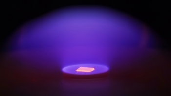 An artificial diamond being grown in a lab at Arizona State University. Trevor Thornton, a professor of electrical engineering in the Ira A. Fulton Schools of Engineering at ASU, is working with an interdisciplinary team of colleagues at ASU and Northrop Grumman Mission Systems to research the use of diamond and boron nitride in transistors. Photo courtesy Franz Koeck/ASU Download Full Image
Thornton’s team is conducting their research through ASU’s Advanced Materials, Processes, and Energy Devices Science and Technology Center, or AMPED STC. AMPED’s goal is to develop materials and technologies with industry partners to support the mission of Arizona’s New Economy Initiative.
The New Economy Initiative aims to improve Arizona’s competitiveness in developing advanced technology. AMPED specifically looks to develop technologies and materials used in the construction of batteries, solar electricity generation and power electronics, which convert electricity to a needed form when it’s moved through transmission channels.
The research team includes Thornton and other ASU faculty members including Terry Alford, a professor of materials science and engineering, Stephen Goodnick, a professor of electrical engineering, and Robert Nemanich, a Regents Professor of physics, as well as doctoral students in electrical engineering and materials science and engineering. They are working with Northrop Grumman Mission Systems as the industry partner for this project.
Diamond efficiency shines
Thornton explains that diamond is under investigation as a material for transistors because of its high thermal conductivity. Thermal conductivity refers to how well a material can dissipate heat.
He gives an analogy of a cool metal surface, which represents high thermal conductivity, and cotton, which represents low thermal conductivity.
“If you put your hand on a metal surface, the metal surface usually feels cool, whereas if you put your hand on a cotton duvet, it immediately feels warm,” Thornton says. “That’s because the metal conducts heat away from your hand very quickly, and so your hand is being cooled, whereas the duvet is keeping your body heat in.”
Thornton says that diamond’s thermal conductivity is highly efficient compared to current materials. Diamond’s thermal conductivity, for example, is eight to 10 times more efficient than gallium nitride. Harnessing diamond to its full potential could shrink the size of transistors by 90%.
Diamond also has a high breakdown field. This means that the material can handle a large amount of voltage relative to most materials before failure. A high breakdown field is ideal for applications that handle large amounts of power.
While diamond is the research team’s chosen material for the main body of a transistor, they are investigating the use of boron nitride, a chemical compound of boron and nitrogen, for the transistors’ electrical contacts.
Like diamond, boron nitride has a high breakdown field and high thermal conductivity. Goodnick’s portion of the research is primarily concerned with computer modeling and simulation of the use of boron nitride transistors.
The research team expects that by combining their knowledge of how diamond and boron nitride work as transistor materials, they can create transistors made from both materials. The team’s hope is that the materials complement each other and work even better together than individually.
“Ultra-wide bandgap semiconductor materials like diamond and boron nitride are expected to lead to more efficient energy conversion using less power with much smaller components,” Goodnick says. “This improves the future energy grid, which is essential for the ongoing transition toward renewable energy and electrification of the transportation sector.”
Better heat dissipation to improve communication
This research has applications that would be especially useful to communications technologies. Many satellites run on solar power, which requires transistors to turn the electricity into a form usable by the satellite.
“You can’t launch a power substation into space,” Thornton says. “Any improvement on size and weight in a satellite has a huge impact.”
Another communications technology the transistors could improve is a bit closer to home: cell phone towers. Transistors convert power to the proper form needed to produce radio frequency waves that cellphones use.
Thornton says that one of the biggest challenges faced when designing and operating cellphone towers is keeping them cool. This is especially the case in a hot environment like Phoenix.
The power transistors in older cellphone towers are typically made from silicon, while those in newer 5G systems will use gallium nitride. Thanks to its improved heat dissipation, Thornton’s team expects transistors made from diamond and boron nitride to greatly reduce the cooling power needed for cell towers. This makes the task of keeping cell towers from overheating far easier.
Shrinking substations
While the project with Northrop Grumman Mission Systems focuses on communications technology, transistors made from diamond and boron nitride also have applications in power conversion for electrical systems and for the electricity grid. These more efficient materials could reduce the size requirements for electricity grid substations.
Substations convert electricity into a usable form for homes and businesses. Typically, they take up an area of land the size of a building.
“If you wander around your neighborhood, sometimes there will be a big transformer surrounded by wires with signs warning you of death,” Thornton says. “That’s a substation. We’d like to make them smaller and more efficient.”
Nemanich, a faculty member in the ASU Department of Physics, leads a group conducting research on power electronics called the ULTRA Energy Frontier Research Center. He also leads a lab for growing artificial diamond material. These materials will be used by Thornton’s team in their research.
“We have been growing diamond for electronic devices for the last 10 years,” Nemanich says. “We believe our diamond deposition lab has unique capabilities for the development of electronic materials and devices.”
An interdisciplinary effort
In addition to Thornton’s electrical engineering expertise and Nemanich’s work with diamond as an electronic material, Alford, a faculty member in the School for Engineering of Matter, Transport and Energy, part of the Fulton Schools, provides his expertise on materials science.
Alford is working on materials characterization, or analyzing the properties of the materials the team is investigating. He also leads a part of the research looking into the use of new types of metallic electrical contacts connected to diamond as a substrate, and he co-advises a materials science and engineering doctoral student involved in the research with Thornton.
“I had done work on silicide, making electrical contacts on silicon, but I never worked on diamond,” Alford says. “I thought this would be a good opportunity to learn about diamond semiconductors.”
Working with Thornton’s team at the AMPED STC has given Alford the chance to conduct research that differs from his normal topics. He believes that his perspective as a materials scientist can help the team achieve its goals.
“I think we bring to the table a desire to understand the impact of a material’s defects,” Alford says. “We want to be able to understand those defects and how they impact a device’s performance.”
Looking to the future of electronics
The transistor research project is funded for two years through the AMPED STC partnership with Northrop Grumman Mission Systems. However, to fully realize the transistors’ potential for widespread applications, Thornton says it could take longer.
“We’ll have breakthroughs, but I don’t see it being widely adopted in the way we’re talking about for five to 10 years,” he says. “It’s that kind of medium- to long-term research of which some applications will happen quicker, while others will be 10 years for widespread consumer applications.”
Communications Specialist, Ira A. Fulton Schools of Engineering
480-965-1314 tjtriolo@asu.edu
Editor’s note: This is the final installment of a four-part series profiling the researchers who work on ASU’s compact X-ray free electron laser. Read the previous installments: Q&As with Regents Professor Petra Fromme, CXFEL Labs Chief Scientist William Graves and CXFEL Labs Director Robert Kaindl.As an undergraduate, Sam Teitelbaum viewed physics very narrowly. “Now I realize th…
Editor’s note: This is the final installment of a four-part series profiling the researchers who work on ASU’s compact X-ray free electron laser. Read the previous installments: Q&As with Regents Professor Petra Fromme, CXFEL Labs Chief Scientist William Graves and CXFEL Labs Director Robert Kaindl.
As an undergraduate, Sam Teitelbaum viewed physics very narrowly.  Assistant Professor Sam Teitelbaum Download Full Image
“Now I realize that physics is a tool you can take with you anywhere, a mindset you can use to approach lots of different problems,” he says.
Teitelbaum brings this approach to his work building compact X-ray equipment in Arizona State University’s Biodesign Institute. An assistant professor in the Department of Physics and a key member of the Biodesign Center for Applied Structural Discovery, Teitelbaum is helping guide the design of the Compact X-ray Free Electron Laser, or CXFEL.
In this Q&A, Teitelbaum recounts his influences and passions, his journey to ASU and how some of his big questions about physics as an undergraduate student are coming full circle with the CXFEL.
Question: What is your role with CXFEL Labs?
Answer: Formally, I am responsible for the design of the quantum materials applications in the CXFEL proposal. I’m also responsible for a subset of the CXFEL laser systems, specifically the overtaking geometry.
Informally, I’m on hand as an experimentalist that likes to troubleshoot things. That means on a day-to-day basis, I’m usually down in the CXFEL Labs helping students working on the lasers or building out the instruments, and just being around to help. There’s a gravitational pull to being down in the labs. There are so many instruments, and unlike a big national lab, you can work with all of them and teach students how to use them. It’s a really fun place to be.
Q: What expertise do you bring to the team?
A: My research uses things like free electron lasers, tabletop lasers and synchrotrons to understand how materials transform. Take water for example — ice melts when it heats up. But temperature is just random motion of atoms, energy deposited into a material as noise. And it takes time for that noise to build up. Using our instruments, we could learn a lot about the properties of matter by observing it on the very fast time scales their individual molecules operate on. We could potentially make materials go through transformations called phase transitions that are so fast that you can’t even say a temperature exists, because there wasn’t enough time for that noise to build up. Can we make new phases of matter by taking advantage of the idea that materials don’t need a temperature?
So what I bring to CXFEL is my experience as an experimentalist to guide our design of the compact X-ray light source and adapt the experiments I’ve conducted with tabletop lasers and synchrotrons to our work here.
Q: How did your academic career prepare you for your work at the CXFEL Labs?
A: I did my PhD at MIT, where I worked on shaping laser pulses to basically arrive at the right place at the right time to better study materials. Typically, when we do these experiments, we want the material to come back to how it was before the laser pulse hit it, because we want to repeat the experiment millions of times. If it won’t come back to its previous state, you need to find a way to get all the information required from one laser pulse.
It turns out the same kind of techniques that I was using to get all the information about materials in one laser pulse are also what we’re using to build the laser undulator at CXFEL. Making laser pulses do gymnastics is an extraordinarily useful concept, which allows us to do everything from manipulating materials to extracting useful information from them.
Q: What has been one challenge in the CXFEL project and how are you and the team overcoming it?
A: CXFEL is a tool that combines two concepts in a novel way: inverse Compton scattering and emittance exchange. Emittance exchange allows us to precisely shape an electron bunch in a way so it emits its X-rays all at once. Inverse Compton scattering is using a high-power laser to make X-rays from our electron beam.
The emittance exchange portion of that puts pretty stringent requirements on the electron beam. Getting all of it to work requires the laser to do new and unique things, which means exciting design challenges that bring our whole team together. This is an area where ASU’s approach has really been key. CXFEL has a smaller team than other XFELs. Getting it to work requires really close collaboration between the laser scientists, accelerator physicists, engineers and even the users to get the most out of our source. We have a lot of developments happening in parallel, which is challenging, but also an opportunity for us to come up with innovative ways to approach problems.
Q: Why is ASU the right place to build these instruments?
A: When you have a project like this that spans different disciplines and departments, there’s a lot of potential for friction. But we all work together very well. At ASU, faculty seem to understand that our work is about raising the quality of the institution as a whole and not necessarily about the prestige of their individual research programs. There’s an understanding that we need to ensure that ASU is doing something interesting and challenging, so we can continue to attract great people and do more interesting and challenging things.
Q: What was the moment when you discovered your passion for science?
A: When I started college at the University of Maryland, I had a professor for electricity and magnetism named Victor Yakovenko. He was a theoretical condensed matter physicist. On day one, he came into class with a little bowl of liquid nitrogen, a high temperature superconductor called yttrium barium copper oxide, and a magnet. He put the superconductor in the liquid nitrogen, which takes it below its critical temperature. He then placed the magnet over the superconductor, where it levitated. And what he said was, “Nobody knows why this material can do this at this temperature.”
I didn’t know that physics had problems like that. I loved the idea that there were these little rocks all over the place, and for the most part, we had no clue how they worked. I was hooked on that.
Now, some of the key experiments that we have in mind for the quantum materials applications of CXFEL are to investigate that very material — yttrium barium copper oxide.
Q: What were other pivotal moments in your career that led you to where you are today?
A: I became really interested in lasers as an undergraduate, but I never got a chance to do all that much undergraduate research on materials. Then in graduate school, I was able to apply that passion for complex materials that started in Professor Yakovenko’s class. Then my postdoctoral work came about basically because I had questions about problems I was working on. I felt that optical lasers couldn’t see the things about materials that I really wanted to see. After learning about what people were doing with XFELs, I just really wanted to be able to answer those questions and see those things that you really need X-rays for. The majority of crystal motion is not easily accessible with optical lasers. In order for an optical laser to observe crystal vibration, it can only see things where every cell in the crystal is doing the same thing at the same time. Which, if you think about all the different arrangements of vibrations that can happen, that’s a very, very, very small fraction of them.
Q: You described physics as a “tool you can take with you anywhere.” Do you apply that mindset to your personal interests or hobbies? Do those interests complement your work?
A: You do end up seeing physics everywhere you go. I love cycling, and one of the fun things about cycling is it’s really easy to do all your own repairs on your bike. A bike is a machine where you can easily see all the moving parts and how they work together. But I also really like cycling because I can turn my brain off and not think about physics for a while. I think we all need a little time away from work. Cooking is something I love, and it has a long intersection with chemistry, which is what I studied as an undergrad. You can use chemistry to inform your cooking and understand why certain recipes work and others don’t.
On the other hand, my background in visual art and theater has really helped my work as a scientist. Both of those were really helpful for honing my communication skills and teaching me to have fun presenting my work. If you can’t explain what you’re doing as a scientist in a clear and engaging way, you’re not going to be able to collaborate with anyone, you’re not going to be able to train anyone, and it will make obtaining grants and awards that much harder.
Q: What motivates and excites you most about your work?
A: Working with students. One of the nice things about being a faculty member is you’re constantly reminded of what it was like to learn this stuff the first time, and I think that really prevents me from becoming cynical about my work.
Q: What potential application or aspect of the CXFEL is most exciting to you?
A: So, yttrium barium copper oxide, the high temperature superconductor I mentioned earlier? Most of the “action” that makes superconductivity that we’re interested in is in the copper and the oxygen atoms of the crystal. CXFEL will be able to see electrons shuffling across those chemical bonds, between the oxygen and copper atoms in real time. We will be able to see what happens when you apply a strong laser field to a high temperature superconductor.
It’s predicted that there are new states of matter in these materials that only exist when the laser fields are on, and we can only see them with a machine like CXFEL. I think it potentially could break open a whole new area because we’ll be seeing new things, and seeing new things changes the way we think about the world.
Q: Who has had the biggest impact/influence on you as a person?
A: My parents. My dad was a biochemist at the EPA and now he is a physician’s assistant, and my mom is a doctor of occupational health. Both of my parents really instilled in me a love of the natural world, curiosity and gave me freedom to explore. I’d like to thank them for letting me clean up my Legos at my own pace and accepting that I had a plan for that pile of Legos. That probably sounds awfully familiar to my colleagues nowadays. “No, no don’t clean it up. I have a plan for that setup!”
The Biodesign Institute and its CXFEL Labs are partially supported by Arizona’s Technology and Research Initiative Fund. TRIF investment has enabled hands-on training for tens of thousands of students across Arizona’s universities, thousands of scientific discoveries and patented technologies, and hundreds of new startup companies. Publicly supported through voter approval, TRIF is an essential resource for growing Arizona’s economy and providing opportunities for Arizona residents to work, learn and thrive.
The Biodesign Institute and its CXFEL Labs are partially supported by Arizona’s Technology and Research Initiative Fund. TRIF investment has enabled hands-on training for tens of thousands of students across Arizona’s universities, thousands of scientific discoveries and patented technologies, and hundreds of new startup companies. Publicly supported through voter approval, TRIF is an essential resource for growing Arizona’s economy and providing opportunities for Arizona residents to work, learn and thrive.
Assistant director of content strategy, Knowledge Enterprise
480-727-5631 pzrioka@asu.edu
Contact us